Flash memory was named because of its NAND chip arrangement. The memory cells are erased in one step as well as "Flash ". Both NAND and Flash memory were developed in the laboratory of Professor Fujio Masuoka from Toshiba in 1984. The term "Flash" was coined because the erasure process of memory data recalls a flash in the camera.
The flash memory type is a type of non-volatile memory that is able to be erased electronically and then rewritten; this means it doesn't require electricity to keep the information stored on the chip.
You can find more about the flash programmers for 8-32 bit custom mcus & spi flash memory via online sources.
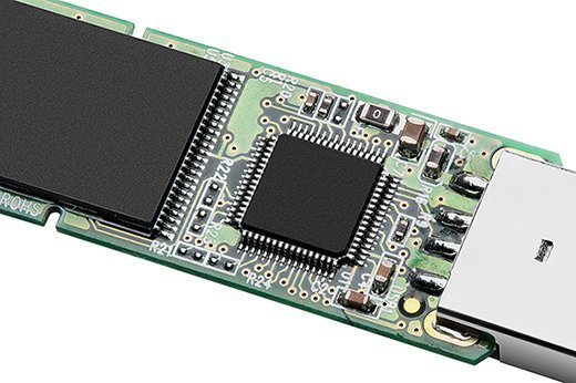
Image Source: Google
Furthermore, flash memory has fast read access times as well as better durability against shock than disks. This is the reason for the increasing popularity of flash memory in applications like storage for batteries-powered devices.
Flash memory is an advanced form of EEPROM (Electrically-Erasable Programmable Read-Only Memory) that allows multiple memory locations to be erased or written in one programming operation.
Contrary to an EPROM (Electrically Programmable Read-Only Memory) an EEPROM can be erased and programmed several times using electricity. The normal EEPROM can only allow one area at the same moment to erase or write to, so flash is able to operate at greater speeds than the system is able to read and write to various locations simultaneously.
In relation to the kind of logic gate that is used inside each storage cell. Flash memory comes in two types and is referred to as flash, NOR flash, and flash.